| CPC C03B 23/203 (2013.01) [C03B 23/02 (2013.01); C25D 3/12 (2013.01); H01L 33/0095 (2013.01); H01L 33/56 (2013.01); C03B 2215/41 (2013.01); C03B 2215/46 (2013.01)] | 23 Claims |

|
1. A method for producing a patterned glass wafer for packaging electronic devices in a wafer assembly, comprising:
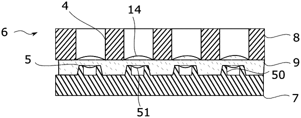
placing a glass sheet between a first mold half and a second mold half, wherein the first mold half has an array of projections and the second mold half has an array of recesses, and wherein the first and second mold halves are configured so that the recesses and projections oppose each other; and
heating until the glass sheet softens while the first and second mold halves are pressed against one another so that the glass sheet is reshaped and forms the patterned glass wafer with the projections introducing cavities into the glass sheet, wherein the glass of the glass sheet opposite the cavities flows into the recesses, wherein the recesses are deep enough for the glass to at least partially not make contact therewith and so as to form a convexly shaped glass surface in each of the recesses, and wherein each projection of the array of projections has a central recess so that each projection of the array of projections has an annular shape so as to form a biconvex lens at each central recess.
|