| CPC B81B 3/0072 (2013.01) [B81C 1/00182 (2013.01); B81C 1/00198 (2013.01); B81B 2203/033 (2013.01); B81C 2201/019 (2013.01)] | 12 Claims |

|
1. A process of manufacturing a MEMS device from a work body of semiconductor material, the process comprising:
forming a buried cavity in the work body;
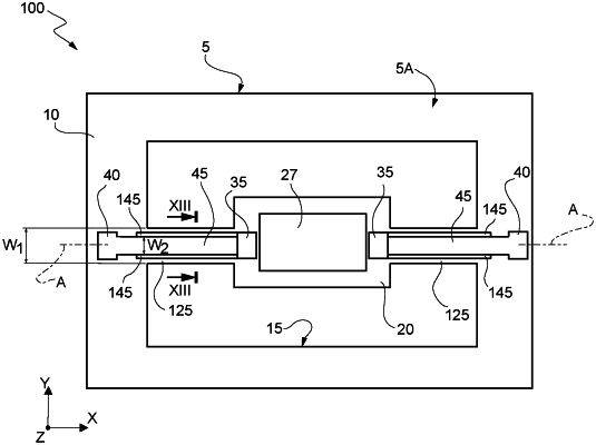
forming a pass-through cavity in the work body, the pass-through cavity defining a support structure surrounding the pass-through cavity;
forming a movable structure suspended in the pass-through cavity;
forming an elastic structure extending in the pass-through cavity between the support structure and the movable structure and along a rotation axis of the MEMS device, wherein the buried cavity is formed to extend longitudinally within the elastic structure to separate a first portion of the elastic structure from a second portion of the elastic structure;
forming a metal region on the first portion of the elastic structure such that a width of the metal region along an axis transverse to both the rotation axis and an axis perpendicular to the rotation axis is less than a width of the elastic structure along the axis perpendicular to the rotation axis;
performing an etching on the elastic structure so that the buried cavity communicates laterally with the pass-through cavity.
|