| CPC B28D 5/0064 (2013.01) [B24B 27/0633 (2013.01); B28D 5/0082 (2013.01); B28D 5/045 (2013.01); H01L 21/67092 (2013.01); H01L 21/67253 (2013.01); B23D 59/00 (2013.01); B28D 5/00 (2013.01); B28D 5/0058 (2013.01); B28D 5/007 (2013.01); B28D 5/04 (2013.01); B28D 7/00 (2013.01); H01L 21/0201 (2013.01)] | 11 Claims |

|
1. A method for producing semiconductor wafers from a workpiece by processing the workpiece by means of a wire saw, comprising:
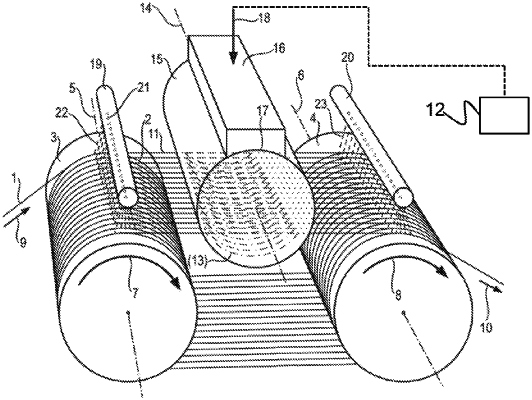
feeding the workpiece through an arrangement of wires which are tensioned between wire guide rollers while being divided into wire groups and move in a running direction;
producing kerfs when the wires engage the workpiece;
for each of the wire groups, determining a placement error of the kerfs of the wire group; and
for each of the wire groups, inducing a compensating movement of the wires of the wire group independently of other wire groups as a function of the determined placement error of the kerfs of the wire group, in a direction perpendicular to a running direction of the wires of the wire group during the feeding of the workpiece through the arrangement of wires, by activating at least one wire group drive element.
|