| CPC B24B 37/013 (2013.01) [B24B 37/042 (2013.01)] | 6 Claims |

|
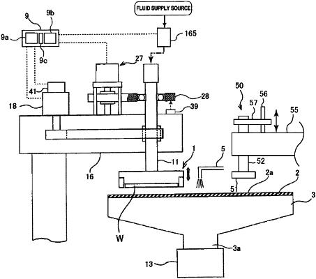
1. A polishing apparatus comprising:
a polishing table configured to support a polishing pad;
a plurality of film thickness sensors embedded in the polishing table, the film thickness sensors outputting a plurality of signals corresponding to a film thickness of a substrate comprising a notch formed on a peripheral edge portion of the substrate; and
a controller configured to measure film thickness information of the substrate based on the signals acquired from the film thickness sensors wherein the film thickness sensors comprise PSD sensors and wherein the PSD sensors emit light to the substrate wherein the signals output from the film thickness sensor comprise a voltage corresponding to an angle of a light reflected from the substrate,
wherein when an inner region on the polishing pad in contact with a peripheral edge portion of the substrate is defined as an inner edge portion and an outer region on the polishing pad in contact with the peripheral edge portion of the substrate is defined as an outer edge portion, the film thickness sensors are arranged from the inner edge portion to the outer edge portion at corresponding positions on the polishing table, and
wherein the controller is further configured to:
analyze film thickness distribution information of the substrate on the measured film thickness information in relation to a position of the notch on the substrate, and
output visualization information of a film thickness distribution with the position of the notch as a reference position, and wherein the position of the notch is determined relative to the film thickness sensors during polishing the substrate and the position of measured film thickness on the substrate is calculated in relation to the notch to the film thickness sensors.
|