| CPC H10K 77/111 (2023.02) [H10K 50/8426 (2023.02)] | 18 Claims |
|
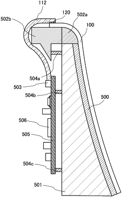
1. A display device comprising:
a first display panel comprising a light-emitting portion; and
a second display panel overlapping the first display panel, the second display panel comprising a light-emitting portion and a region transmitting visible light adjacent to the light-emitting portion, wherein a light-transmitting layer is provided between the region transmitting visible light of the second display panel and the light-emitting portion of the first display panel, and
wherein one of the first display panel and the second display panel is fixed to a member having a curved surface with a metal plate provided therebetween.
|