| CPC H10K 71/00 (2023.02) [H10K 50/84 (2023.02); H10K 50/86 (2023.02); H10K 59/12 (2023.02); H10K 77/10 (2023.02)] | 16 Claims |
|
1. A method for manufacturing a display device, the method comprising:
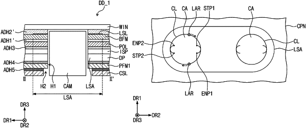
preparing a panel which comprises a display panel, a polarizing film disposed on the display panel, and a first adhesive disposed on the polarizing film and on which a cutoff area defined as a cutoff line having a closed curve is defined; and
irradiating a first intense light toward the cutoff line to cut portions of the display panel and the polarizing film, which overlap the cutoff area,
wherein the first intense light is provided along the cutoff line from a first start point to a first end point, the first start point is disposed inside the cutoff line, and the first end point is provided at different point from the first start point.
|