| CPC H10K 71/00 (2023.02) [H01L 21/31051 (2013.01); H01L 21/31127 (2013.01)] | 15 Claims |
|
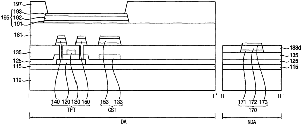
1. A display device comprising:
a planarization layer covering transistors in a display area on a substrate;
an organic light emitting diode on the planarization layer;
a pad electrode in a non-display area on the substrate, the non-display area surrounding the display area; and
a capping layer capping a side surface of the pad electrode, the capping layer including a material different from that of the planarization layer, wherein
the pad electrode includes a first laver on the substrate, a second layer on the first layer, and a third layer on the second layer,
the capping layer does not extend directly under the planarization layer,
the capping layer does not overlap a top surface of the pad electrode,
the capping layer covers side surfaces of the first and second layers of the pad electrode, and does not cover at least a part of a side surface of the third layer of the pad electrode,
the capping layer has a flat top surface lower than the top surface of the pad electrode, and
the capping layer is a remnant of a different layer than that of the planarization layer.
|