| CPC H10K 59/80522 (2023.02) [H10K 59/1201 (2023.02); H10K 59/122 (2023.02); H10K 59/80515 (2023.02); H10K 59/80521 (2023.02); H10K 59/873 (2023.02); H10K 59/8792 (2023.02); H10K 71/00 (2023.02)] | 17 Claims |

|
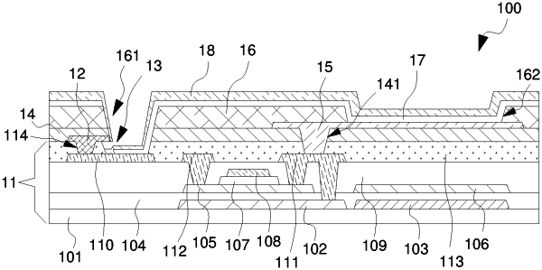
1. A display panel, comprising:
an array substrate comprising a source electrode, a drain electrode, a first auxiliary electrode, and a protective layer disposed on the first auxiliary electrode, wherein the first auxiliary electrode, the source electrode, and the drain electrode are formed of a same material on a same layer;
a second auxiliary electrode disposed on the protective layer and connected to the first auxiliary electrode;
an undercut structure formed on the protective layer, extending to directly below the second auxiliary electrode, and exposing the first auxiliary electrode;
a flat layer disposed on the second auxiliary electrode and the protective layer;
an anode electrode disposed on the flat layer;
a pixel defining layer disposed on the anode electrode and the flat layer, and provided with a first opening connected to the undercut structure;
an organic light-emitting layer disposed on the pixel defining layer and not completely covering an exposed part of the first auxiliary electrode; and
a cathode electrode disposed on the organic light-emitting layer, extending into the undercut structure, and connected to the first auxiliary electrode;
wherein the array substrate further comprises:
a base substrate;
a light-shielding metal layer disposed directly on the base substrate,
a first electrode plate disposed directly on the base substrate, wherein the light-shielding metal layer and the first electrode plate are disposed in a same layer;
a buffer layer disposed on the light-shielding metal layer and the first electrode plate;
an amorphous oxide semiconductor layer disposed directly on the buffer layer; and
a second electrode plate disposed directly on the buffer layer, wherein the amorphous oxide semiconductor layer and the second electrode plate are disposed in a same layer;
wherein the first electrode plate and the second electrode plate form a capacitor structure;
wherein the undercut structure has a depth into the second auxiliary electrode of 0.1 μm to 1 μm.
|