| CPC H10K 59/38 (2023.02) [G02F 1/133512 (2013.01); G02F 1/133516 (2013.01); H10K 50/865 (2023.02); H10K 59/122 (2023.02); H10K 71/00 (2023.02)] | 17 Claims |

|
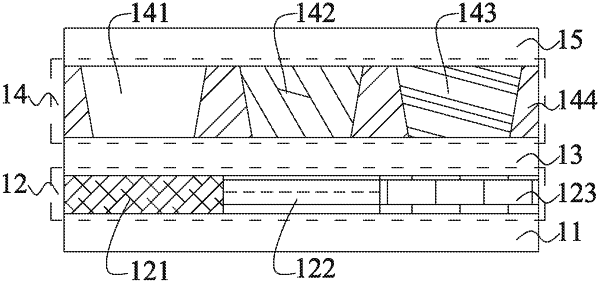
1. A color filter substrate, comprising a first substrate, a color resist layer, an overcoat layer, and a quantum dot layer, which are sequentially stacked along a first direction;
wherein the color resist layer is provided with a plurality of sub-color resist layers with different colors arranged along a second direction, and there is no black matrix disposed between two adjacent sub-color resist layers; and
the quantum dot layer is divided into a plurality of quantum dot areas arranged along the second direction, a plurality of banks are disposed between and correspond to two adjacent quantum dot areas, and the banks are black;
wherein the banks have a predetermined transmittance t within a visible light range, the predetermined transmittance t of the banks is less than 5% when a wavelength of ambient light L is greater than 350 nm and less than 510 nm, and the predetermined transmittance t of the banks is greater than 90% when the wavelength of ambient light L is greater than 650 nm.
|