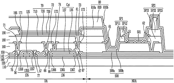
| CPC H10K 59/131 (2023.02) [H10K 50/814 (2023.02); H10K 50/844 (2023.02)] | 22 Claims |

|
1. A display device comprising:
a substrate including a display area and a non-display area which is adjacent to the display area;
a common voltage transmitting line disposed in the non-display area and including a first common voltage transmitting line and a second common voltage transmitting line which overlaps the first common voltage transmitting line;
a first insulating layer disposed between the first common voltage transmitting line and the second common voltage transmitting line; and
an auxiliary electrode disposed on the common voltage transmitting line,
wherein the second common voltage transmitting line defines a first opening overlapping the first insulating layer, and
wherein the auxiliary electrode contacts the first insulating layer through the first opening and overlaps at least one of the first common voltage transmitting line, the second common voltage transmitting line, and the first insulating layer.
|