| CPC H10K 59/131 (2023.02) [G09G 3/3283 (2013.01); H10K 59/1213 (2023.02); H10K 59/1216 (2023.02); G09G 2300/0426 (2013.01); G09G 2300/0842 (2013.01); G09G 2320/0233 (2013.01); H01L 27/1225 (2013.01); H01L 27/124 (2013.01); H01L 27/1251 (2013.01); H01L 27/1255 (2013.01); H01L 29/78675 (2013.01); H01L 29/7869 (2013.01)] | 26 Claims |
|
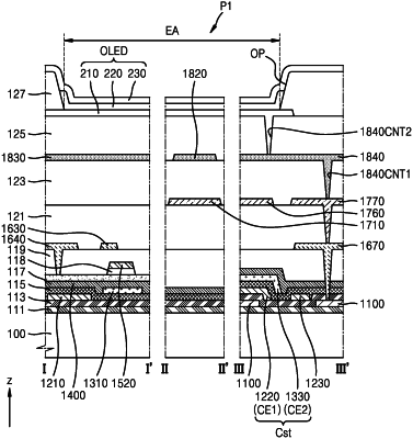
1. A display apparatus comprising:
a first semiconductor layer disposed on a substrate;
a first gate layer disposed on the first semiconductor layer, the first gate layer including a driving gate electrode;
a second gate layer disposed on the first gate layer, the second gate layer including a capacitor upper electrode;
a first connecting electrode layer disposed on the second gate layer, the first connecting electrode layer including a transfer wiring;
a second connecting electrode layer disposed on the first connecting electrode layer, the second connecting electrode layer including a horizontal connection wiring extending in a first direction;
a third connecting electrode layer disposed on the second connecting electrode layer, the third connecting electrode layer including a vertical connection wiring extending in a second direction that intersects the first direction;
a light-emitting diode including a pixel electrode disposed on the vertical connection wiring; and
an insulating layer disposed between the vertical connection wiring and the pixel electrode of the light-emitting diode.
|