| CPC H10K 59/124 (2023.02) [H01L 29/786 (2013.01); H10K 59/1213 (2023.02); H10K 59/122 (2023.02); H10K 59/131 (2023.02); H10K 71/00 (2023.02); H10K 2102/00 (2023.02)] | 16 Claims |

|
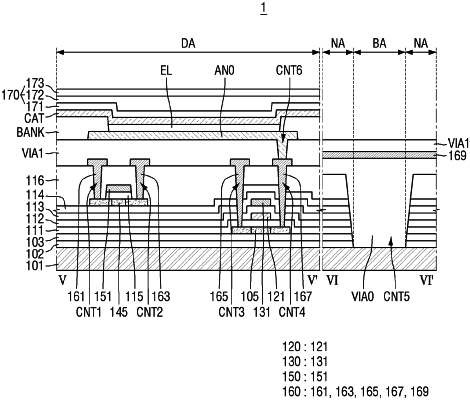
1. A display device comprising:
a substrate including a display area and a non-display area around the display area;
a first insulating layer disposed on the substrate;
a second insulating layer disposed on the first insulating layer;
a first semiconductor layer disposed on the second insulating layer;
a third insulating layer on the first semiconductor layer;
a first gate electrode on the third insulating layer;
a fourth insulating layer disposed on the first gate electrode;
a second gate electrode on the fourth insulating layer;
a fifth insulating layer on the second gate electrode;
a sixth insulating layer on the fifth insulating layer;
a second semiconductor layer on the sixth insulating layer;
an seventh insulating layer on the second semiconductor layer;
a third gate electrode on the seventh insulating layer;
a eighth insulating layer on the third gate electrode;
a first source electrode or a second drain electrode on the eighth insulating layer; and
a third source electrode or a fourth drain electrode on the eighth insulating layer, wherein
a material of the fifth insulating layer is different from a material of the sixth insulating layer,
the first source or the second drain electrode is electrically connected to the first semiconductor layer,
the third source electrode or the fourth drain electrode is electrically connected to the second semiconductor layer,
the fifth insulating comprises silicon nitride (SiNx),
wherein the sixth insulating layer comprises silicon oxide (SiOx),
the first semiconductor layer includes crystal silicon, and
the second semiconductor layer includes an oxide.
|