| CPC H10K 59/124 (2023.02) [H10K 59/1213 (2023.02)] | 8 Claims |
|
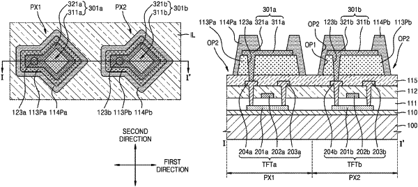
1. A display apparatus comprising:
a substrate;
a thin film transistor on the substrate and comprising a semiconductor layer and a gate electrode;
a first insulating layer on the substrate and covering the semiconductor layer and the gate electrode of the thin film transistor;
a second insulating layer on the first insulating layer and at least partially covering a top surface of an electrode connected to the semiconductor layer of the thin film transistor;
a third insulating layer on the second insulating layer, an opening defined in the third insulating layer extends to a top surface of the second insulating layer;
a pixel electrode positioned on the third insulating layer and electrically connected to the thin film transistor by contacting the electrode; and
a fourth insulating layer on the third insulating layer covering an edge of the pixel electrode and a side surface of the third insulating layer,
wherein the opening of the third insulating layer surrounds the entire edge of the pixel electrode in a plan view,
wherein the electrode connected to the semiconductor layer contacts a top surface of the first insulating layer,
wherein the fourth insulating layer covers the entire side surface of the third insulating layer and the top surface of the second insulating layer, in the opening of the third insulating layer, and
wherein the second insulating layer does not have a hole in the opening of the third insulating layer.
|