| CPC H10K 59/124 (2023.02) [H10K 50/822 (2023.02); H10K 59/122 (2023.02); H10K 77/10 (2023.02)] | 18 Claims |

|
1. A display device comprising:
a base substrate including a display region in which image display is performed;
a frame region disposed on a periphery of the display region;
a non-display region having an island shape inside the display region;
a thin film transistor layer including a first interlayer insulating film and a second interlayer insulating film that are disposed on the base substrate and are sequentially stacked;
a light-emitting element layer disposed on the thin film transistor layer and in which a plurality of light-emitting elements is arranged in correspondence with a plurality of subpixels configuring the display region; and
a sealing film disposed on the light-emitting element layer and including at least one layer of a sealing insulating film, wherein:
a first electrode, a function layer, and a second electrode are sequentially stacked in each of the plurality of light-emitting elements,
a through-hole extending through the base substrate in a thickness direction of the base substrate is formed in the non-display region,
a separation wall is provided in a frame shape along a circumferential edge of the through-hole in the non-display region,
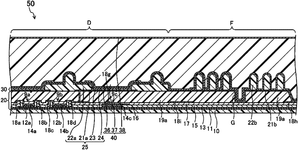
the separation wall includes a wall base portion provided in a frame shape by a part of the second interlayer insulating film, and a resin layer provided in an eave shape on the wall base portion to protrude toward a through-hole side and a display region side,
an opening portion opening upward are provided on peripheries of the wall base portion on the through-hole side and the display region side in the second interlayer insulating film,
the function layer includes a common function layer that is disposed to be common to the plurality of subpixels, and
the common function layer is disposed on the resin layer to extend from the display region to the through-hole and is cut apart below circumferential ends of the resin layer on the through-hole side and the display region side.
|