| CPC H10K 59/122 (2023.02) [H10K 50/84 (2023.02); H10K 50/865 (2023.02); H10K 59/38 (2023.02); H10K 71/00 (2023.02); H10K 59/1201 (2023.02)] | 16 Claims |

|
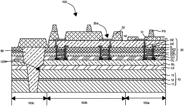
1. A display device, comprising:
a transparent display region;
a main display region adjacent to the transparent display region;
a substrate;
a pixel defining layer disposed on the substrate and defined with openings, wherein the pixel defining layer comprises a first pixel defining layer and a second pixel defining layer, the first pixel defining layer is positioned in the transparent display region, the second pixel defining layer is positioned in the main display region, and an absorbance of the first pixel defining layer is less than an absorbance of the second pixel defining layer; and
light-emitting pixels disposed in the openings,
wherein a ratio of the absorbance of the first pixel defining layer to the absorbance of the second pixel defining layer ranges from one-half to two-thirds,
wherein an absolute value of a difference between a reflectance of the first pixel defining layer and a reflectance of the second pixel defining layer is less than or equal to two percent.
|