| CPC H10K 59/1213 (2023.02) [G09G 3/3233 (2013.01); H10K 59/1216 (2023.02); H10K 59/131 (2023.02); H10K 71/00 (2023.02); G09G 2300/0809 (2013.01); H01L 27/1222 (2013.01); H01L 27/124 (2013.01); H01L 27/1255 (2013.01); H01L 27/127 (2013.01); H01L 29/66757 (2013.01); H01L 29/78675 (2013.01); H10K 59/1201 (2023.02)] | 5 Claims |

|
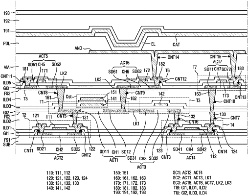
1. A method of manufacturing a display device including a first transistor, a second transistor, and a third transistor disposed on different layers, respectively, the method comprising:
forming a first semiconductor layer on a substrate, the first semiconductor layer including a semiconductor pattern of the first transistor;
forming a first gate insulating film on the first semiconductor layer;
forming a first conductive layer on the first gate insulating film, the first conductive layer including a gate electrode of the first transistor;
forming a first interlayer insulating film on the first conductive layer;
forming an upper surface of the first interlayer insulating film substantially flat;
forming a second semiconductor layer on the upper surface of the first interlayer insulating film, the second semiconductor layer including a semiconductor pattern of the second transistor;
forming a second gate insulating film on the second semiconductor layer;
forming a second conductive layer on the second gate insulating film, the second conductive layer including a gate electrode of the second transistor and a first electrode of a capacitor electrically connected to the gate electrode of the second transistor;
forming a second interlayer insulating film on the second conductive layer;
forming a third conductive layer on the second interlayer insulating film, the third conductive layer including a second electrode of the capacitor;
forming a third interlayer insulating film on the third conductive layer;
forming a contact pattern penetrating the third interlayer insulating film and connected to the second semiconductor layer;
forming a semiconductor connection portion on the third interlayer insulating film and contacting an upper surface of the contact pattern;
forming a third semiconductor layer on the same layer as the semiconductor connection portion, the third semiconductor layer including a semiconductor pattern of the third transistor;
forming a third gate insulating film on the third semiconductor layer; and
forming a fourth conductive layer on the third gate insulating film, the fourth conductive layer including a gate electrode of the third transistor.
|