| CPC H10K 50/844 (2023.02) [H10K 59/12 (2023.02); H10K 59/65 (2023.02); G02F 1/133331 (2021.01); H10K 50/818 (2023.02); H10K 50/828 (2023.02); H10K 50/8426 (2023.02); H10K 50/865 (2023.02); H10K 50/868 (2023.02); H10K 59/1216 (2023.02); H10K 59/122 (2023.02); H10K 59/124 (2023.02); H10K 59/38 (2023.02); H10K 59/40 (2023.02)] | 25 Claims |

|
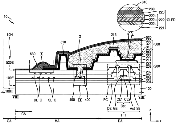
1. A display panel comprising:
a substrate comprising a first area, a second area at least partially surrounding the first area, and an intermediate area between the first area and the second area;
an insulating layer on the substrate;
a plurality of display elements in the second area, and each comprising a pixel electrode, an opposite electrode, and an intermediate layer between the pixel electrode and the opposite electrode;
a groove in the intermediate area;
a thin-film encapsulation layer covering the plurality of display elements, and comprising an inorganic encapsulation layer and an organic encapsulation layer; and
an inorganic layer over the thin-film encapsulation layer,
wherein at least one sub-layer in the intermediate layer comprises a first portion and a second portion that are disposed in the intermediate area and disconnected around the groove to be separated from each other, one of the first portion and a second portion of the at least one sub-layer is disposed in the groove, and the inorganic layer directly contacts the insulating layer beyond an edge of the at least one sub-layer and an edge of the inorganic encapsulation layer that are located in the intermediate area.
|