| CPC H10K 50/818 (2023.02) [H10K 59/124 (2023.02); H10K 59/131 (2023.02); H10K 71/00 (2023.02); H10K 71/621 (2023.02); H10K 59/1201 (2023.02); H10K 59/126 (2023.02); H10K 2102/3026 (2023.02)] | 20 Claims |
|
1. A display device comprising:
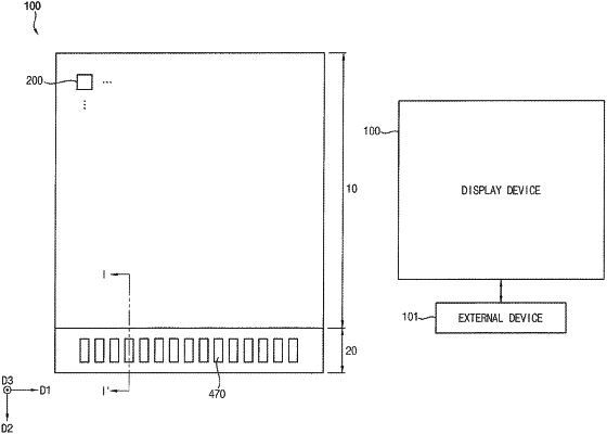
a substrate comprising a display area and a pad area;
a lower electrode in the display area on the substrate, the lower electrode comprising:
a first electrode, the first electrode comprising titanium (Ti) and being formed by a first etching process,
a second electrode on the first electrode, the second electrode comprising a first metal other than titanium (Ti) and being formed by a second etching process different from the first etching process, and
a third electrode on the second electrode, the third electrode comprising a second metal other than titanium (Ti) and being formed by the second etching process,
a light emitting layer over the first electrode;
an upper electrode on the light emitting layer; and
a pad electrode in the pad area on the substrate.
|