| CPC H10K 50/818 (2023.02) | 19 Claims |
|
1. A light-emitting device comprising:
a first electrode;
a second electrode facing the first electrode;
an emission layer located between the first electrode and the second electrode; and
a charge transport region located between the emission layer and the first electrode,
wherein:
light emitted from the emission layer passes to the outside through the second electrode;
the first electrode is a reflective electrode;
the first electrode comprises a transparent layer and a reflective layer; and
Equation 1, Equation 2, and Equation 4 are satisfied as follows:
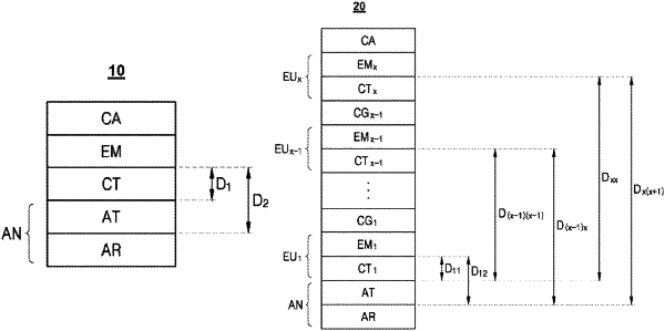
L1−a1≤D1≤L1+a1 Equation 1
wherein, in Equation 1, D1 is a distance between i) an interface between the transparent layer of the first electrode and the charge transport region and ii) an interface between the emission layer and the charge transport region, L1 is a first resonance distance of light emitted from the emission layer, and a1 is a real number in a range of about 0 nanometers (nm) to about 50 nm,
L2−a2≤D2≤L2+a2 Equation 2
wherein, in Equation 2, D2 is a distance between a) an interface between the reflective layer of the first electrode and the transparent layer of the first electrode and b) an interface between the emission layer and the charge transport region, L2 is a second resonance distance of light emitted from the emission layer, and a2 is a real number in a range of about 0 nm to about 50 nm, and
n1−n2≥0.1 Equation 4
wherein, in Equation 4, n1 is a refractive index of the transparent layer of the first electrode, and n2 is a refractive index of a layer in direct contact with the transparent layer of the first electrode from among layers comprised in the charge transport region.
|