| CPC H10K 50/131 (2023.02) [H10K 50/165 (2023.02); H10K 59/122 (2023.02); H10K 59/38 (2023.02)] | 20 Claims |

|
1. A display device comprising:
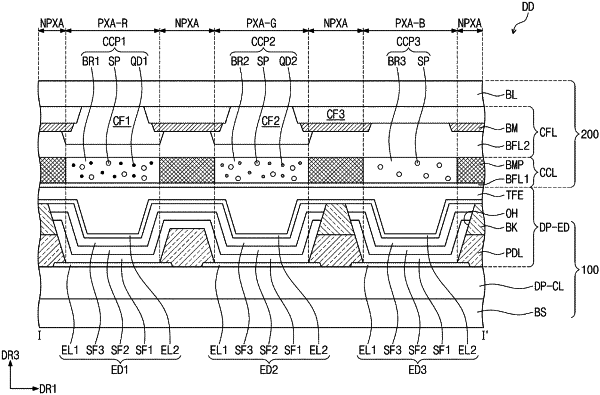
an upper display substrate comprising a first pixel region configured to emit a first light having a first wavelength region, a second pixel region configured to emit a second light having a second wavelength region different from the first wavelength region of the first light, and a third pixel region configured to emit a third light having a third wavelength region different from the first wavelength region of the first light and the second wavelength region of the second light; and
a lower display substrate comprising a first light-emitting element disposed to overlap the first pixel region, a second light-emitting element disposed to overlap the second pixel region, and a third light-emitting element disposed to overlap the third pixel region, and
wherein the second light-emitting element comprises one or more first stacks configured to emit the second light, the one or more first stacks comprising a plurality of organic layers,
the third light-emitting element comprises one or more second stacks configured to emit the third light, the one or more second stacks comprising a plurality of organic layers,
the one or more first stacks comprise a first hole transport region, a first emission layer, and a first electron transport region,
the one or more second stacks comprise a second hole transport region, a second emission layer, and a second electron transport region, and
a concentration of a conductive material included in the first electron transport region is higher than a concentration of a conductive material included in the second electron transport region.
|