| CPC H10B 63/34 (2023.02) | 20 Claims |
|
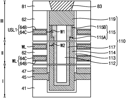
1. A semiconductor device comprising:
a horizontal wiring layer on a substrate;
a stack structure disposed on the horizontal wiring layer, the stack structure comprising a plurality of insulating layers and a plurality of electrode layers alternately stacked on each other; and
a pillar structure extending into the horizontal wiring layer and extending through the stack structure,
wherein the plurality of electrode layers comprise
one or a plurality of selection lines adjacent to an uppermost end of the stack structure, and
a plurality of word lines surrounding the stack structure below the one or plurality of selection lines,
wherein the pillar structure comprises
a variable resistive layer,
a channel layer between the variable resistive layer and the stack structure,
a gate dielectric layer between the channel layer and the stack structure, and
a blocking pattern disposed between the variable resistive layer and the channel layer and being adjacent to a first selection line among the one or plurality of selection lines, wherein the channel layer is disposed between the first selection line and the blocking pattern.
|