| CPC H10B 43/27 (2023.02) [H01L 29/0649 (2013.01); H10B 41/27 (2023.02); H10B 41/30 (2023.02); H10B 43/30 (2023.02)] | 2 Claims |

|
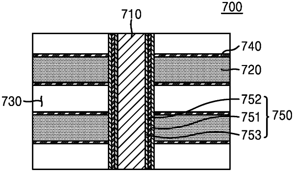
1. A 3-dimensional (3D) flash memory comprising:
at least one channel layer formed to extend in a first direction;
a plurality of electrode layers formed to extend in a second direction orthogonal to a first direction so as to be vertically stacked with respect to the at least one channel layer;
a plurality of air gaps between the plurality of electrode layers to separate the plurality of electrode layers from each other;
at least one oxide-nitride-oxide (ONO) layer comprising a first oxide layer, a nitride layer, and a second oxide layer and formed to extend in the first direction to connect the at least one channel layer and the plurality of electrode layers; and
a blocking material layer formed on an upper portion and a lower portion of each of the plurality of electrode layers,
wherein the first oxide layer, the nitride layer, and the second oxide layer extend continuously in the first direction between the at least one channel layer and each of the plurality of electrode layers and the plurality of air gaps, and
wherein the first oxide layer contacts the plurality of air gaps, the blocking material layer, and the plurality of electrode layers.
|