| CPC H10B 43/27 (2023.02) | 47 Claims |

|
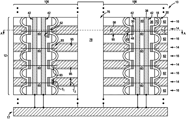
1. An integrated assembly, comprising:
a stack of alternating insulative levels and conductive levels;
a pillar of channel material extending through the stack, the conductive levels having terminal regions adjacent the pillar and laterally offset from the pillar;
charge-storage-material-segments adjacent the conductive levels of the stack, and being between the channel material and the terminal regions; vertically-neighboring charge-storage-material-segments being spaced from one another by intervening regions aligned with the insulative levels;
tunneling material between the charge-storage-material-segments and the channel material;
charge-blocking-material between the charge-storage-material-segments and the terminal regions; and
ribbons of dielectric material extending vertically across the insulative levels and being laterally inset relative to the terminal regions; the ribbons having first regions adjacent the conductive levels and having second regions between the first regions; the second regions being laterally inset relative to the first regions such that innermost surfaces of the ribbons have convex configurations.
|