| CPC H10B 43/27 (2023.02) [G11C 16/10 (2013.01); H01L 21/31116 (2013.01); H01L 23/528 (2013.01); H01L 23/53257 (2013.01); H01L 23/53261 (2013.01); H01L 29/1037 (2013.01); H01L 29/7926 (2013.01); H10B 43/20 (2023.02); H10B 43/35 (2023.02); A45F 5/021 (2013.01); B24B 3/54 (2013.01); B26B 29/025 (2013.01)] | 20 Claims |

|
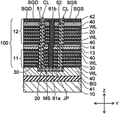
1. A semiconductor memory device, comprising:
a source layer;
a first unit provided above the source layer, the first unit including at least a source-side selection gate layer;
a second unit stacked above the first unit, the second unit including a plurality of first electrode layers as control gates of memory cells, the first electrode layers being alternately stacked in a stacking direction with a plurality of first insulating layers therebetween;
a bit line provided above the second unit;
a first columnar part piercing the first unit in the stacking direction, the first columnar part including a first channel body with a tubular configuration and a first core insulator part provided inside the first channel body with the tubular configuration; and
a second columnar part piercing the second unit in the stacking direction, the second columnar part including a second channel body with a tubular configuration and a second core insulator part provided inside the second channel body with the tubular configuration, wherein
the first channel body and the second channel body are formed as one body and are connected with each other in the stacking direction, and
a central axis of the first columnar part piercing the first unit is shifted in a direction perpendicular to the stacking direction from a central axis of the second columnar part piercing the second unit.
|