| CPC H10B 43/27 (2023.02) [H01L 23/5226 (2013.01); H10B 41/10 (2023.02); H10B 41/27 (2023.02); H10B 41/40 (2023.02); H10B 43/10 (2023.02); H10B 43/40 (2023.02)] | 20 Claims |
|
1. A three-dimensional semiconductor memory device, comprising:
a substrate including a cell array region and a connection region;
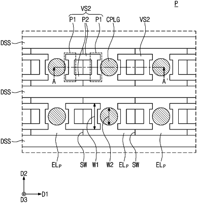
an electrode structure including electrodes vertically stacked on the substrate, the electrodes including respective pad portions on the connection region, and the pad portions of the electrodes being stacked in a staircase structure along a first direction;
contact plugs coupled to the pad portions of the electrodes, respectively;
first vertical structures penetrating the electrode structure on the cell array region; and
second vertical structures penetrating the electrode structure on the connection region, each of the second vertical structures including:
a dielectric pillar having a sidewall in direct contact with the electrodes,
at least two first parts spaced apart from each other in the first direction, and
second parts spaced apart from each other in a second direction that intersects the first direction, the second parts connecting the at least two first parts to each other to define a single second vertical structure that is between adjacent contact plugs in the first direction, and the first and second directions being parallel to a top surface of the substrate,
wherein each of the pad portions of the electrodes has a first width in the second direction, and
wherein the single second vertical structure has a second width less than the first width in the second direction,
wherein each of the contact plugs is between directly adjacent single second vertical structures.
|