| CPC H10B 43/27 (2023.02) [H01L 23/5283 (2013.01); H10B 41/10 (2023.02); H10B 41/27 (2023.02); H10B 41/35 (2023.02); H10B 41/40 (2023.02); H10B 43/10 (2023.02); H10B 43/35 (2023.02); H10B 43/40 (2023.02)] | 20 Claims |
|
1. A three-dimensional (3D) memory device, comprising:
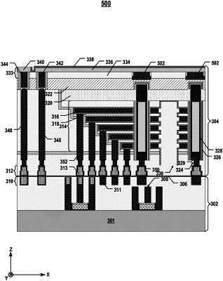
a memory stack comprising interleaved conductive layers and dielectric layers on a first side of a semiconductor layer;
a plurality of channel structures each extending vertically through the memory stack and in contact with the first side of the semiconductor layer;
a plurality of source contacts in contact with a second side of the semiconductor layer opposite to the first side;
a plurality of contacts through the semiconductor layer; and
a backside interconnect layer on the second side of the semiconductor layer and comprising a source line mesh in a plan view, wherein the plurality of source contacts and a first set of the plurality of contacts are in contact with the source line mesh.
|