| CPC H10B 43/10 (2023.02) [H10B 41/10 (2023.02); H10B 41/27 (2023.02); H10B 43/27 (2023.02); G11C 16/0483 (2013.01); H10B 41/35 (2023.02); H10B 43/35 (2023.02)] | 40 Claims |

|
1. A method used in forming a memory array comprising strings of memory cells, comprising:
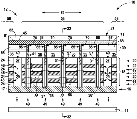
forming a stack comprising vertically-alternating insulative tiers and conductive tiers having channel-material strings therein;
forming walls above an insulating material that is directly above the channel-material strings, a void space disposed laterally-between those of the walls that are immediately-laterally-adjacent one another and that comprises a longitudinal outline of individual digitlines to be formed, spaced openings being in the insulating material directly below the void space;
relative to the walls, selectively depositing a conductive metal nitride in the void space, in the spaced openings, and atop the insulating material laterally-between the walls and the spaced openings to form a lower portion of the individual digitlines laterally-between the immediately-adjacent walls, the conductive metal nitride that is in individual of the spaced openings being directly electrically coupled to individual of the channel-material strings; and
forming a conductive material in the void space directly above and directly electrically coupled to the lower portion of the individual digitlines to form an upper portion thereof.
|