| CPC H10B 41/41 (2023.02) [G11C 16/0483 (2013.01); G11C 16/10 (2013.01); G11C 16/26 (2013.01); H01L 23/5283 (2013.01); H10B 41/27 (2023.02); H10B 41/35 (2023.02); H10B 41/40 (2023.02); H10B 43/27 (2023.02); H10B 43/35 (2023.02); H10B 43/40 (2023.02)] | 20 Claims |

|
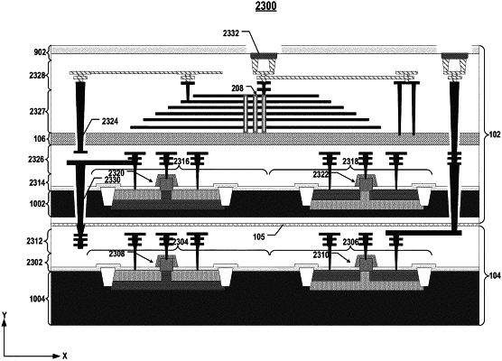
1. A three-dimensional (3D) memory device, comprising:
a first semiconductor structure, comprising:
an array of NAND memory strings;
a first peripheral circuit of the array of NAND memory strings, the first peripheral circuit comprising a first transistor;
a polysilicon layer between the array of NAND memory strings and the first peripheral circuit, the polysilicon layer being in contact with sources of the array of NAND memory strings; and
a first semiconductor layer in contact with the first transistor;
a second semiconductor structure, comprising:
a second peripheral circuit of the array of NAND memory strings, the second peripheral circuit comprising a second transistor; and
a second semiconductor layer in contact with the second transistor; and
a bonding interface between the first semiconductor structure and the second semiconductor structure,
wherein the second peripheral circuit is between the bonding interface and the second semiconductor layer; and
the first semiconductor layer is between the polysilicon layer and the second semiconductor layer.
|