| CPC H10B 41/40 (2023.02) [H01L 23/481 (2013.01); H01L 24/80 (2013.01); H01L 25/0657 (2013.01); H01L 25/50 (2013.01); H10B 41/27 (2023.02); H10B 41/35 (2023.02); H10B 43/27 (2023.02); H10B 43/35 (2023.02); H10B 43/40 (2023.02); H01L 2224/80001 (2013.01)] | 19 Claims |
|
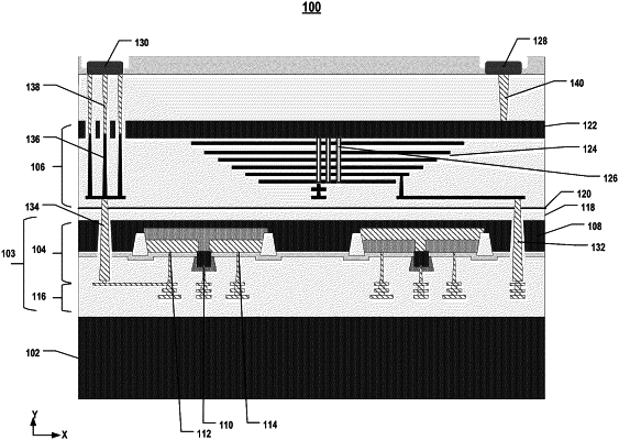
1. A three-dimensional (3D) memory device, comprising:
a first semiconductor structure comprising a peripheral device;
a second semiconductor structure disposed on the first semiconductor structure, the second semiconductor structure comprising a doped semiconductor layer, and a memory array structure disposed between the doped semiconductor layer and the first semiconductor structure, the peripheral device in the first semiconductor structure facing opposite to the second semiconductor structure; and
a contact structure, wherein the second semiconductor structure is disposed between the contact structure and the first semiconductor structure, the doped semiconductor layer is disposed between the contact structure and the memory array structure, and a first contact pad is formed on the contact structure electrically coupled to the doped semiconductor layer of the second semiconductor structure.
|