| CPC H10B 12/30 (2023.02) [H10B 12/03 (2023.02); H10B 12/482 (2023.02)] | 9 Claims |
|
1. A semiconductor structure manufacturing method, comprising:
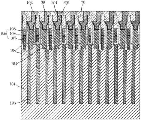
providing a substrate, wherein the substrate comprises a plurality of active area structures, a plurality of bit line structures on the plurality of active area structures, an insulating layer on the plurality of bit line structures, and a plurality of first hole structures distributed at intervals and penetrating through the insulating layer;
forming a barrier layer on side walls and bottom walls of the plurality of first hole structures and a top surface of the insulating layer;
forming a first conductive layer on the barrier layer, wherein the plurality of first hole structures are filled with the barrier layer and the first conductive layer;
removing the first conductive layer and the barrier layer outside the plurality of first hole structures to make top surfaces of the first conductive layer and the barrier layer flush with the top surface of the insulating layer;
forming a first supporting layer with patterns on the first conductive layer, the barrier layer and the insulating layer, wherein the first supporting layer with patterns exposes part of the top surface of the insulating layer, part of the first conductive layer and part of the barrier layer;
etching the part of the first conductive layer and the part of the barrier layer with the first supporting layer with patterns as a mask, to form a plurality of first pad structures in the plurality of first hole structures, and a plurality of second hole structures in the first supporting layer and the first hole structures, wherein the plurality of first pad structures are electrically connected to the plurality of active area structures, respectively;
depositing a second supporting layer in the plurality of second hole structures, wherein the plurality of second hole structures are filled with the second supporting layer, and the second supporting layer covers the part of the top surface of the insulating layer;
removing the first supporting layer with patterns, and forming a plurality of third hole structures in the second supporting layer; and
forming a plurality of second pad structures in the plurality of third hole structures, wherein the plurality of second pad structures are connected to the plurality of first pad structures, respectively.
|