| CPC H10B 12/00 (2023.02) [H01L 27/1207 (2013.01); H01L 27/1225 (2013.01); H01L 27/124 (2013.01); H01L 27/1255 (2013.01); H01L 29/78648 (2013.01); H01L 29/7869 (2013.01)] | 12 Claims |
|
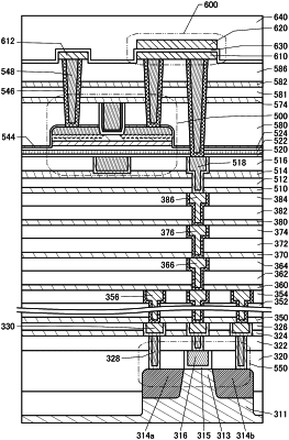
1. A memory device comprising n memory cells (n is an integer greater than or equal to 3), n first wirings, n second wirings, and a third wiring,
wherein an i-th memory cell (i is an integer greater than or equal to 2 and less than n) comprises a first transistor[i], a second transistor[i], and a capacitor[i],
wherein an i−1-th memory cell comprises a first transistor[i−1], a second transistor[i−1], and a capacitor[i−1],
wherein an i+1-th memory cell comprises a first transistor[i+1], a second transistor[i+1], and a capacitor[i+1],
wherein a gate of the first transistor[i] is electrically connected to an i-th first wiring,
wherein a source of the first transistor[i] is electrically connected to a drain of the first transistor[i−1],
wherein a drain of the first transistor[i] is electrically connected to a source of the first transistor[i+1],
wherein a gate of the second transistor[i] is electrically connected to the drain of the first transistor[i],
wherein a source of the second transistor[i] is electrically connected to a drain of the second transistor[i−1],
wherein a drain of the second transistor[i] is electrically connected to a source of the second transistor[i+1],
wherein a back gate of the second transistor[i] is electrically connected to an i-th second wiring,
wherein a back gate of the second transistor[i−1] is electrically connected to an i−1-th second wiring,
wherein a back gate of the second transistor[i+1] is electrically connected to an i+1-th second wiring,
wherein the capacitor[i] is between the gate of the second transistor[i] and the third wiring,
wherein the capacitor[i−1] is between a gate of the second transistor[i−1] and the third wiring, and
wherein the capacitor[i+1] is between a gate of the second transistor[i+1] and the third wiring.
|