| CPC H05K 5/0095 (2013.01) [A61N 1/3787 (2013.01); H02J 50/10 (2016.02); H05K 1/181 (2013.01); H05K 5/0052 (2013.01); H05K 2201/10015 (2013.01)] | 20 Claims |
|
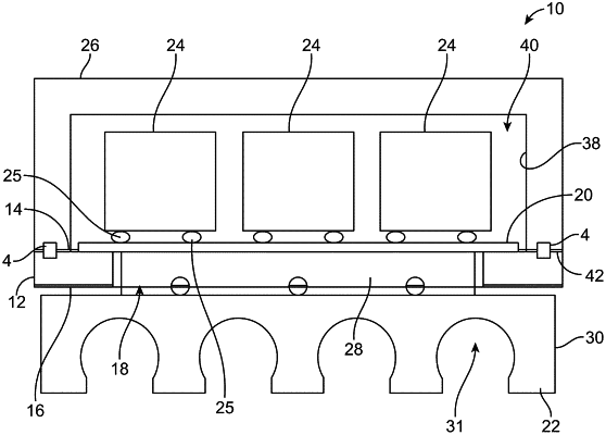
1. An electronic package comprising:
a nonconductive substrate comprising a first major surface, a second major surface, and an opening disposed through the substrate between the first major surface and the second major surface;
a conductive layer hermetically sealed to the first major surface of the substrate and over the opening;
a conductor block disposed in the opening and extending beyond the second major surface of the substrate, wherein the conductor block is electrically connected to the conductive layer;
an electronic device disposed adjacent to the first major surface of the substrate and electrically connected to the conductive layer; and
a nonconductive cover disposed over the electronic device and the nonconductive substrate and hermetically sealed to the substrate, wherein the electronic device is disposed within a cavity of the cover.
|