| CPC H04W 24/10 (2013.01) [H04L 5/0048 (2013.01); H04L 5/14 (2013.01); H04W 52/34 (2013.01); H04W 76/28 (2018.02)] | 26 Claims |

|
1. A user equipment (UE) for wireless communication, comprising:
a memory; and
one or more processors, coupled to the memory, configured to:
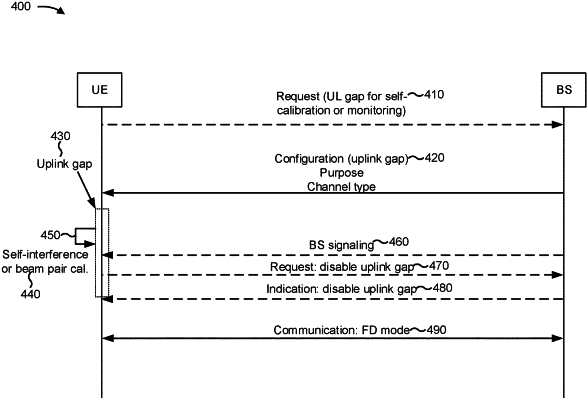
receive configuration information indicating an uplink gap;
transmit a reference signal in the uplink gap;
receive, from a base station, signaling in the uplink gap; and
perform, based at least in part on the reference signal and the signaling in the uplink gap, at least one of a self-interference measurement or a beam pair calibration for full-duplex communication,
wherein the self-interference measurement or the beam pair calibration is a first purpose for the uplink gap, and wherein the configuration information indicates the first purpose and a second purpose for the uplink gap.
|