| CPC H04N 25/778 (2023.01) [H01L 27/14612 (2013.01); H04N 25/766 (2023.01)] | 10 Claims |
|
1. A solid state imaging element, comprising:
a driving circuit configured to supply a specific reference signal, wherein a level of the specific reference signal gradually fluctuates with lapse of time; and
a plurality of pixels, wherein each of the plurality of pixels includes:
a change amount acquisition section;
an auto-zero transistor configured to initialize the change amount acquisition section to obtain a brightness change amount;
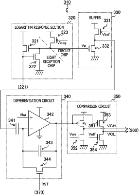
a logarithm response section configured to obtain a logarithm value of a photoelectric current;
a differentiation circuit configured to differentiate the logarithm value and output the differentiated logarithm value as a differentiated signal;
a comparison circuit configured to compare the differentiated signal with a specific threshold; and
a reset control section configured to switch, based on occurrence of a specific address event, the auto-zero transistor by use of the specific reference signal.
|