| CPC H04N 25/772 (2023.01) [H03F 3/45269 (2013.01); H03M 1/38 (2013.01); H04N 25/78 (2023.01); H03F 2200/129 (2013.01); H03F 2200/135 (2013.01)] | 8 Claims |
|
1. An imaging device comprising:
a plurality of pixel circuits that each generates a pixel signal including a pixel voltage corresponding to an amount of received light, and performs AD conversion by comparing the pixel signal with a reference signal; and
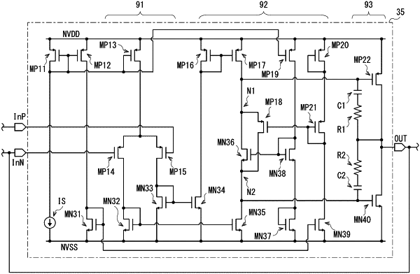
a reference signal generator including a signal generation circuit and a voltage follower circuit, the signal generation circuit that generates a voltage signal having a ramp waveform, and the voltage follower circuit that performs a voltage follower operation on a basis of the voltage signal to generate the reference signal, and supplies the reference signal to the plurality of pixel circuits,
wherein the voltage follower circuit includes an amplifier having a positive input terminal that is supplied with the voltage signal, a negative input terminal, an output terminal that is coupled to the negative input terminal and outputs the reference signal, and an output circuit coupled to the output terminal,
wherein the output circuit includes
a first transistor of a first electrical conductivity type having a source coupled to a first power supply node, a drain coupled to the output terminal, and a gate, and
a second transistor of a second electrical conductivity type having a source coupled to a second power supply node, a drain coupled to the output terminal, and a gate, and
wherein the amplifier includes a first differential transistor pair that is coupled to the positive input terminal and the negative input terminal, and generates a differential current including a first current and a second current.
|