US 12,081,889 B2
Image sensor including CMOS image sensor pixel and dynamic vision sensor pixel
Yunjae Suh, Incheon (KR); Junseok Kim, Hwaseong-si (KR); Hyunsurk Ryu, Hwaseong-si (KR); Keun Joo Park, Seoul (KR); and Masamichi Ito, Hwaseong-si (JP)
Assigned to SAMSUNG ELECTRONICS CO., LTD., Suwon-si (KR)
Filed by SAMSUNG ELECTRONICS CO., LTD., Suwon-si (KR)
Filed on Apr. 7, 2023, as Appl. No. 18/297,233.
Application 18/297,233 is a continuation of application No. 17/492,059, filed on Oct. 1, 2021, granted, now 11,637,983.
Application 17/492,059 is a continuation of application No. 16/552,299, filed on Aug. 27, 2019, granted, now 11,140,349, issued on Oct. 5, 2021.
Claims priority of application No. 10-2018-0107280 (KR), filed on Sep. 7, 2018; and application No. 10-2019-0028938 (KR), filed on Mar. 13, 2019.
Prior Publication US 2023/0247321 A1, Aug. 3, 2023
Int. Cl. H04N 25/75 (2023.01); H04N 25/47 (2023.01); H04N 25/77 (2023.01)
CPC H04N 25/75 (2023.01) [H04N 25/47 (2023.01); H04N 25/77 (2023.01)] 22 Claims
OG exemplary drawing
 
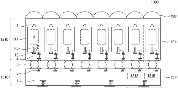
1. A sensor comprising:
a first substrate comprising a plurality of photoelectric conversion devices and a floating diffusion region connected to the plurality of photoelectric conversion devices; and
a second substrate configured to receive charges from the plurality of photoelectric conversion devices via a plurality of metal-to-metal bondings, and to determine a change in light intensity incident on the plurality of photoelectric conversion devices based on the charges,
wherein the first substrate is coupled with the second substrate via the plurality of metal-to-metal bondings, and
wherein the plurality of photoelectric conversion devices form a single dynamic vision sensor pixel.