| CPC H04N 25/75 (2023.01) [H04N 25/701 (2023.01); H04N 25/702 (2023.01); H01L 27/14612 (2013.01)] | 23 Claims |
|
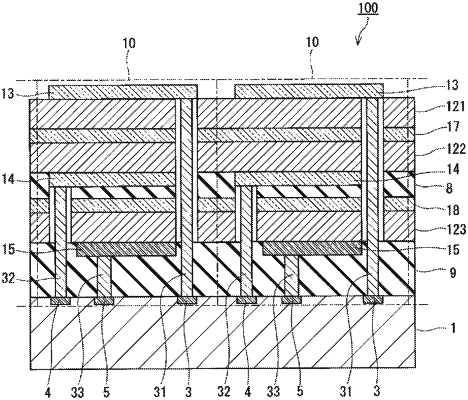
1. An imaging device comprising:
a plurality of pixels, wherein:
each of the plurality of pixels includes:
a first photoelectric conversion layer that converts light into first electric charge,
a first pixel electrode that collects the first electric charge,
a second photoelectric conversion layer that is arranged below the first photoelectric conversion layer and that converts light into second electric charge,
a second pixel electrode that collects the second electric charge,
a third photoelectric conversion layer that is arranged below the second photoelectric conversion layer and that converts light into third electric charge,
a third pixel electrode that collects the third electric charge,
a first counter electrode that is arranged between the first photoelectric conversion layer and the second photoelectric conversion layer, and
a second counter electrode that is arranged between the second photoelectric conversion layer and the third photoelectric conversion layer, and
the first pixel electrode, the first photoelectric conversion layer, the first counter electrode, the second photoelectric conversion layer, the second pixel electrode, the second counter electrode, the third photoelectric conversion layer, and the third pixel electrode are arranged in this order, without interposing any photoelectric conversion layer between the second pixel electrode and the second counter electrode.
|