| CPC H04B 1/10 (2013.01) [H04L 27/0008 (2013.01)] | 20 Claims |

|
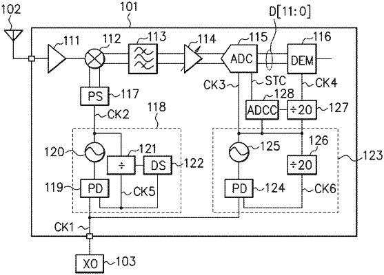
1. A processing circuit, comprising:
a clock generating circuit configured to generate, based on a reference clock signal and a frequency set signal, a first clock signal having a frequency higher than a frequency of the reference clock signal;
a frequency dividing and delay circuit configured to generate a second clock signal having a frequency lower than the frequency of the first clock signal so that the second clock signal has a first phase difference with the reference clock signal by dividing the frequency of the first clock signal and delaying the first clock signal based on a phase shift set signal and the frequency set signal;
an analog-to-digital converter circuit configured to convert an analog signal into a digital signal based on the first clock signal and a conversion trigger signal indicating a sampling period and a conversion period;
a digital signal processing circuit configured to execute processing according to the digital signal based on the second clock signal; and
a control circuit configured to generate the conversion trigger signal so that the conversion trigger signal has the same cycle as the second clock signal based on the frequency set signal and the first clock signal.
|