| CPC H03M 1/365 (2013.01) | 19 Claims |

|
1. An analog-to-digital converter (ADC) for converting an analog signal into a digital signal, the ADC comprising:
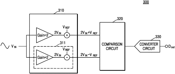
an amplifier circuit configured to receive the analog signal, and to generate a plurality of amplifier signals by amplifying the analog signal;
a comparison circuit configured to compare a plurality of voltage levels corresponding to the plurality of amplifier signals with a positive reference voltage level and a negative reference voltage level, and to output conversion target signals based on a result of the comparison; and
a converter circuit configured to convert the conversion target signals into a plurality of digital signals,
wherein the amplifier circuit is further configured to:
generate a first amplifier signal from among the plurality of amplifier signals by adding the positive reference voltage level to a voltage level of the amplified analog signal, and
generate a second amplifier signal from among the plurality of amplifier signals by subtracting the positive reference voltage level from the voltage level of the amplified analog signal.
|