| CPC H03K 5/13 (2013.01) [H03D 7/00 (2013.01); H04L 25/03057 (2013.01)] | 20 Claims |

|
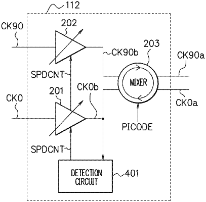
1. A phase interpolation circuit, comprising:
a first buffer circuit configured to adjust at least one of a rise time and a fall time of a first reference clock signal based on a first control signal to generate a first input clock signal;
a second buffer circuit configured to adjust at least one of a rise time and a fall time of a second reference clock signal having a first phase difference from the first reference clock signal based on a second control signal to generate a second input clock signal;
a detection circuit configured to detect at least one of a rise time and a fall time of at least one of the first input clock signal and the second input clock signal and generate the first control signal and the second control signal according to a detection result thereof; and
a mixer circuit configured to generate an output clock signal having a phase between a phase of the first input clock signal and a phase of the second input clock signal based on the first input clock signal and the second input clock signal.
|