| CPC H03K 17/6871 (2013.01) | 16 Claims |

|
1. A FET switch stack comprising:
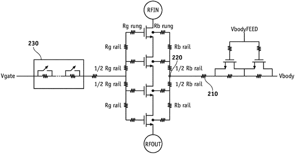
a stacked arrangement of FET switches connected at one end to an RF terminal configured to be coupled to an RF signal, the FET switch stack configured to have an ON or OFF steady state where the FET switches are respectively ON or OFF and a transition state where the FET switches transition from ON to OFF or vice versa;
a gate resistor network comprising resistors connected to gate terminals of the FET switches;
common gate resistors connected to the gate resistor network, the gate resistor network and the common gate resistors configured to feed a gate control voltage to the gate terminals of the FET switches;
a body resistor network comprising resistors connected to body terminals of the FET switches;
common body resistors connected to the body resistor network, the body resistor network and the common body resistors configured to feed a body control voltage to the body terminals of the FET switches;
a stacked arrangement of gate bypass FET switches, each gate bypass FET switch connected across a respective common gate resistor of the common gate resistors and configured to i) bypass the respective common gate resistor during at least a portion of the transition state of the FET switch stack and ii) not to bypass the respective common gate resistor during at least a portion of states of the FET switch stack different from the transition state; and
a stacked arrangement of body bypass FET switches, each body bypass FET switch connected across a respective common body resistor of the common body resistors and configured to i) bypass the respective common body resistor during at least a portion of the OFF steady state of the FET switch stack and ii) not to bypass the respective common body resistor during at least a portion of the ON steady state.
|