| CPC H03K 17/161 (2013.01) | 12 Claims |

|
1. A device, comprising:
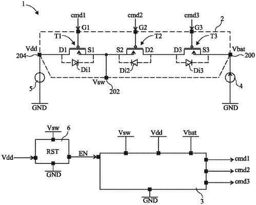
a first terminal configured to connect to a first voltage source supplying a first supply potential referenced to ground;
a second terminal configured to supply a second potential referenced to ground;
a third terminal configured to connect to a second voltage source supplying a third supply potential referenced to ground;
a first PMOS transistor having a source connected to the second terminal and a drain connected to the third terminal;
a second PMOS transistor having a source connected to the second terminal;
a third PMOS transistor having a source connected to the first terminal and a drain connected to the drain of the second PMOS transistor;
a control circuit configured to generate gate control signals for controlling the first, second, and third transistors, the control circuit being configured to receive the first, second, and third supply potentials;
wherein the control circuit comprises:
a first circuit configured to supply a first high reference potential equal to A times the first supply potential and a first low reference potential equal to B times the first supply potential, with A and B positive numbers strictly less than 1, A being greater than B; and
a second circuit configured to supply a second high reference potential equal to C times the second supply potential and a second low reference potential equal to D times the second supply potential, with C and D positive numbers strictly less than 1, C being greater than D.
|