| CPC H03K 17/08122 (2013.01) [H03K 17/6871 (2013.01); H03K 17/74 (2013.01)] | 14 Claims |
|
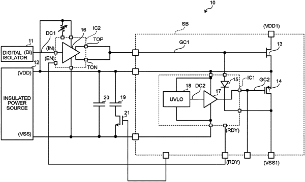
1. An inrush current suppression circuit comprising:
a normally-on transistor;
a normally-off transistor connected in series with the normally-on transistor;
a first drive circuit configured to drive the normally-on transistor;
a second drive circuit configured to drive the normally-off transistor;
a diode connected between an output of the first drive circuit and an output terminal of the normally-off transistor;
a first power source smoothing circuit configured to perform smoothing of a source current to be supplied to the first drive circuit and the second drive circuit; and
a switch circuit configured to switch connection/disconnection of a current path passing through the first power source smoothing circuit.
|