| CPC H03F 3/217 (2013.01) [H03F 2200/451 (2013.01)] | 21 Claims |

|
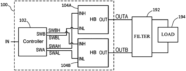
1. A class-D amplifier circuit, comprising:
a circuit board;
a first amplifier output;
a second amplifier output;
a first power device disposed on the circuit board and comprising a left control terminal, a right control terminal, and first and second conduction terminals;
a second power device disposed on the circuit board and comprising first and second conduction terminals;
a third power device disposed on the circuit board and comprising first and second conduction terminals;
a fourth power device disposed on the circuit board and comprising first and second conduction terminals;
a first left driver device disposed adjacent to the left side of the first power device and coupled to the left control terminal of the first power device;
a first right driver device disposed adjacent to the right side of the first power device and coupled to the right control terminal of the first power device,
wherein the first conduction terminal of the first power device and the first conduction terminal of the third power device are coupled to a first power supply voltage,
wherein the second conduction terminal of the first power device and the first conduction terminal of the second power device are coupled to the first amplifier output,
wherein the second conduction terminal of the second power device and the second conduction terminal of the fourth power device are coupled to a second power supply voltage,
wherein the second conduction terminal of the third power device and the first conduction terminal of the fourth power device are coupled to the second amplifier output,
wherein the first power device is a multi-tub power device comprises:
a drain contact corresponding to the first conduction terminal of the first power device;
a plurality of left gate contacts disposed on a left half of the first power device, wherein one of the left gate contacts corresponds to the left control terminal of the first power device;
a plurality of left source contacts disposed on the left half of the first power device;
a plurality of right gate contacts disposed on a right half of the first power device, wherein one of the right gate contacts corresponds to the right control terminal of the first power device; and
a plurality of right source contacts disposed on the right half of the first power device,
wherein at least one of the plurality of left source contacts or the plurality of right source contacts corresponds to the second conduction terminal of the first power device, and
wherein the plurality of left source contacts and the plurality of right source contacts are all coupled to the first amplifier output,
wherein the first left driver device comprises a plurality of Kelvin source connections,
wherein the first right driver device comprises a plurality of Kelvin source connections,
wherein the plurality of left source contacts of the first power device are coupled to the plurality of Kelvin source connections of the first left driver device, and
wherein the plurality of right source contacts of the first power device are coupled to the plurality of Kelvin source connections of the first right driver device.
|