| CPC H03D 7/1458 (2013.01) [H01L 29/78648 (2013.01); H01L 29/7869 (2013.01)] | 8 Claims |

|
1. A semiconductor device comprising a mixer circuit and a bias circuit,
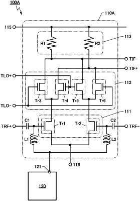
wherein the mixer circuit comprises a voltage-to-current conversion portion, a current switch portion, and a current-to-voltage conversion portion,
wherein the bias circuit comprises a bias supply portion and a first transistor,
wherein the voltage-to-current conversion portion comprises a second transistor and a third transistor,
wherein the bias circuit is configured to output a bias voltage to be supplied to a gate of the second transistor and a gate of the third transistor,
wherein one of a source and a drain of the first transistor is electrically connected to the gate of the second transistor and the gate of the third transistor,
wherein the bias circuit comprises a voltage holding portion electrically connected to the bias supply portion, and a buffer portion electrically connected to the voltage holding portion,
wherein an output of the buffer portion is electrically connected to the gate of the second transistor and the gate of the third transistor,
wherein the voltage holding portion is configured to hold the bias voltage, and
wherein the buffer portion is configured to amplify power of the bias voltage.
|