|
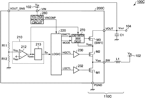
1. A control circuit of a boost DC/DC converter including a high side transistor and a low side transistor, wherein DC/DC standing for direct-current/direct-current, the control circuit comprising: a pulse modulator including a first error amplifier that amplifies an error between a reference voltage and a feedback signal corresponding to an output voltage of the boost DC/DC converter, the pulse modulator being configured to generate a pulse signal with a pulse modulated according to an output signal of the first error amplifier; a logic circuit that generates a high side control signal and a low side control signal based on the pulse signal; and a load switch drive circuit that drives a load switch that is a PMOS transistor connected between the high side transistor and a load, wherein PMOS standing for p-channel metal-oxide semiconductor, wherein the load switch drive circuit is capable of making a switch between (i) a first mode for fully turning on the PMOS transistor and (ii) a second mode for supplying a drive voltage corresponding to the output signal of the first error amplifier to a gate of the PMOS transistor.
|
