| CPC H01S 5/0612 (2013.01) [H01S 5/02453 (2013.01); H01S 5/0261 (2013.01); H01S 5/22 (2013.01); H01S 5/323 (2013.01)] | 14 Claims |

|
1. A laser diode chip comprising:
an n-type semiconductor region, a p-type semiconductor region, and an active layer arranged between the n-type semiconductor region and the p-type semiconductor region, an n-type contact and a p-type contact,
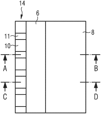
at least one heating element arranged on a side of the laser diode chip facing the p-type semiconductor region, the heating element functioning as a resistance heater, and
at least one metallic seed layer, wherein
the heating element comprises a part of the seed layer,
the p-type contact is arranged on a further part of the seed layer, and
in a longitudinal direction parallel to a longitudinal axis of a waveguide of the laser diode chip, the heating element comprises alternating first regions in which only the seed layer is present and second regions in which an additional metal layer is applied directly to the seed layer, so that the first regions have a higher resistance for a current through the resistance heater than the second regions.
|