| CPC H01S 5/04256 (2019.08) [G03B 21/2033 (2013.01); H01S 5/0261 (2013.01); H01S 5/04254 (2019.08); H01S 5/12 (2013.01); H01S 5/125 (2013.01); H01S 5/18308 (2013.01); H01S 5/34313 (2013.01); H01S 5/34333 (2013.01); H01S 5/4025 (2013.01); G03B 21/2013 (2013.01); G03B 33/12 (2013.01)] | 13 Claims |
|
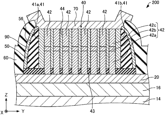
1. A light emitting device comprising:
a substrate;
a light emitting unit positioned above the substrate, the light emitting unit including:
a first semiconductor layer;
a second semiconductor layer having a conductivity type different from a conductivity type of the first semiconductor layer; and
a light emitting layer provided between the first semiconductor layer and the second semiconductor layer;
a first insulating layer provided on a side wall of the light emitting unit; and
a first electrical conducting layer provided on a surface of the first insulating layer, and on a surface of the second semiconductor layer,
wherein the first electrical conducting layer includes:
a first part that contacts the second semiconductor layer and includes a side facing the second semiconductor layer and an opposite side facing away from the second semiconductor layer;
a second part that is provided outside of the first part in a plan view, the second part being inclined with respect to a direction normal to the substrate away from each of the substrate and the opposite side of the first part; and
a third part that is provided outside of the second part in the plan view, the third part being inclined with respect to the direction normal to the substrate toward the substrate and away from the side facing the second semiconductor layer.
|