| CPC H01S 5/02345 (2021.01) [H01S 5/02315 (2021.01); H01S 5/042 (2013.01); H01S 5/0608 (2013.01)] | 19 Claims |
|
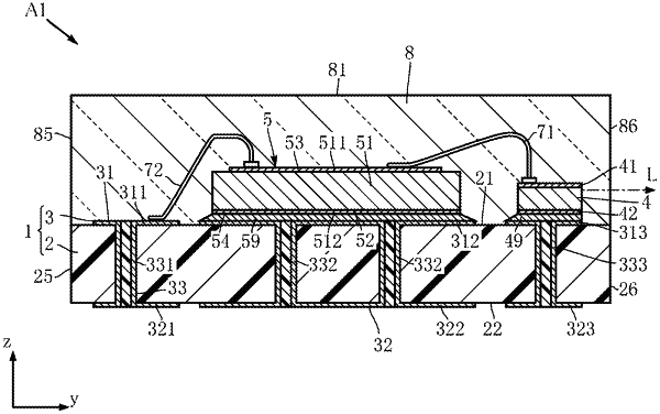
1. A semiconductor laser device comprising:
a semiconductor laser element;
a switching element with a gate electrode, a source electrode and a drain electrode; and
a support member including a conductive part that forms a conduction path to the switching element and the semiconductor laser element and supports the semiconductor laser element and the switching element,
wherein the conductive part has a first section spaced apart from the semiconductor laser element,
the semiconductor laser device further comprising:
at least one first wire connected to the source electrode of the switching element and the semiconductor laser element; and
at least one second wire connected to the source electrode of the switching element and the first section of the conductive part.
|