| CPC H01R 13/6691 (2013.01) [G02B 6/425 (2013.01); H01R 13/50 (2013.01); H01R 13/6581 (2013.01); H01R 43/18 (2013.01); G02B 6/423 (2013.01); G02B 6/4246 (2013.01); G02B 6/4249 (2013.01); G02B 6/428 (2013.01); H01R 13/665 (2013.01); H01R 13/6658 (2013.01); H05K 2201/10121 (2013.01)] | 6 Claims |

|
1. A signal transmission device based on molded interconnect device and laser direct structuring (MID/LDS) technology, comprising:
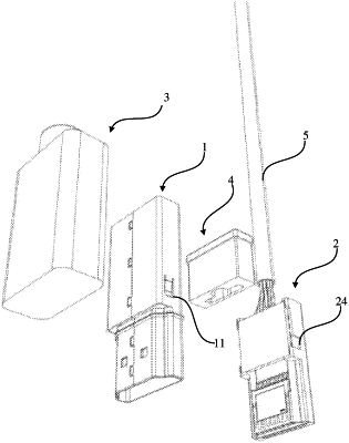
a shielding shell (1), of which two sides are respectively provided with a first buckle (11) and a second buckle (12); and
a photoelectric conversion module (2), including a carrier (21), an electrical module (22) and an optical module (23), wherein a first surface (26) of the carrier (21) is provided with the optical module (23), a second surface (27) of the carrier (21) is provided with the electrical module (22), and two side surfaces of the carrier (21) are respectively provided with a first card slot (24) and a second card slot (25), and wherein the first buckle (11) is buckled into the first card slot (24), and the second buckle (12) is buckled into the second card slot (25), so that the photoelectric conversion module (2) is fixed in the shielding shell (1), and
wherein, the carrier (21) comprises a first connection end (28) and a second connection end (29), the first surface (26) has a first recessed structure (201) at the second connection end (29), the second surface (27) has a second recessed structure (202) at the second connection end (29), wherein a driving chip (211), a photoelectric conversion chip (212) and the optical module (23) are accommodated in the first recessed structure (201), the electrical module (22) is accommodated in the second recessed structure (202), a conductive terminal (215) is provided at the first connection end (28) of the carrier (21), the driving chip (211) and the photoelectric conversion chip (212) are fixed on the first surface (26) of the carrier (21), the driving chip (211), the photoelectric conversion chip (212) and the conductive terminal (215) are electrically connected to each other, and the carrier (21) is integrally formed based on MID/LDS technology;
wherein a positioning hole (214) is arranged on the first surface (26) of the carrier (21), and a conductive silica gel hole (213) is arranged on the second surface (27) of the carrier (21);
wherein the electrical module (22) includes a copper wire (221), an electronic component (222), and an electronic component carrier (223); wherein a conductive sheet (2221) is printed on the electronic component (222), the copper wire (221), the electronic component (222), the conductive sheet (2221) and the conductive terminal (215) are electrically connected in sequence, the electronic component (222) is fixed on the electronic component carrier (223), and the electronic component carrier (223) fixes the electrical module (22) in the second recessed structure (202) of the carrier (21) by connecting to the conductive silica gel hole (213).
|